
Multilayer printed circuit boards (PCBs) are the unsung heroes that power our modern devices. These intricate creations have revolutionized the way we design and manufacture electronics, enabling us to pack more functionality into smaller spaces while maintaining efficiency and reliability.
Let’s dig deeper into the world of multilayer PCBs, exploring what they are, how they work and the benefits they bring to the electronic landscape. If you need multilayer PCBs, be sure to contact Sonic Manufacturing for a free quote.
Understanding Multilayer PCBs
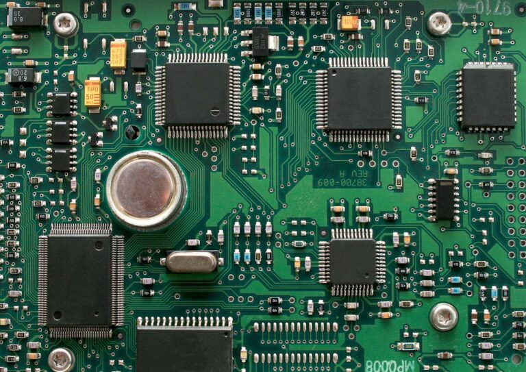
A printed circuit board is essentially a flat board made of an insulating material, such as fiberglass or epoxy resin, with conductive pathways etched onto its surface. These pathways, or traces, allow and direct the flow of electric current between components like integrated circuits (ICs), resistors, capacitors, and more.
While traditional single-layer PCBs serve their purpose well, they have limitations when it comes to complex and compact design. This is where multilayer PCBs come into play. As the name suggests, these boards consist of multiple layers of insulating material sandwiched between layers of conductive material. These layers are bonded together through a process called lamination.
How Multilayer PCBs Work
The magic of multilayer PCBs lies in their ability to provide a greater density of components and connections in a relatively small area. This is crucial for today’s electronics, where devices are becoming smaller and more powerful. The layers in a multilayer PCB are interconnected using vias, which are tiny holes filled with conductive material. Vias allow signals and power to pass through different layers so that the components can communicate and function harmoniously.
The inner layers of a multilayer PCB are often used for power and ground planes. These planes provide stable voltage references and minimize electromagnetic interference, ensuring the reliability and performance of the circuit. The outer layers house most of the components and their interconnections.
Benefits of Multilayer PCBs
- Size efficiency. Multilayer PCBs allow for compact design, which is crucial in devices like smartphones, tablets, and wearables. By stacking components vertically, these boards save valuable space and enable the creation of sleek, lightweight gadgets.
- Improved signal integrity. With multiple layers dedicated to power and ground planes, multilayer PCBs reduce the risk of signal interference and crosstalk. This leads to improved signal quality and overall circuit performance.
- Complexity and functionality. The ability to create intricate connections between components on different layers facilitates the design of complex circuits. This paves the way for devices with advanced features and capabilities.
- Reduced EMI. Electromagnetic interference (EMI) can have a negative impact on the performance of electronic devices. Multilayer PCBs help contain EMI by providing shielding and better signal isolation.
- Reliability. The use of multiple layers enhances the reliability of connections. Redundancy in paths ensures that if one connection fails, there’s often an alternative route for the current to flow.
Multilayer PCBs Power Modern Devices
Multilayer printed circuit boards allow manufacturing of the compact and efficient devices we have today. From smartphones to medical devices and beyond, multilayer PCBs play a pivotal role in shaping our technological landscape. As technology continues to evolve, it’s certain that these ingenious circuit boards will remain at the heart of innovation. To request your free quote, contact Sonic Manufacturing today.