
From the Experts at Sonic Manufacturing Technologies
Printed circuit board (PCB) design is an essential part of electronics design. Having an efficient design layout minimizes the chances of errors and reduces the chances of having to redo the board. Plus, a well-designed PCB layout lessens the probability of signal interference, EMI, and crosstalk.
Sonic Manufacturing Technologies understands the pressures to bring your products to the market quickly, which means there’s no room for error. We will take you from concept to prototype and help you get to market faster with our in-house capabilities. Below are some tips and tricks that we use to ensure an efficient PCB layout for our clients.
Plan the PCB Layout
Before starting the PCB design, it’s essential to plan the layout. The planning stage helps to ensure that the design meets the required specifications and the components fit correctly. At this stage, we’ll decide the size and shape of the board, and the placement of the components. The planning stage also helps to minimize errors and ensures the design is optimized for manufacturability.
Choose the Right Components
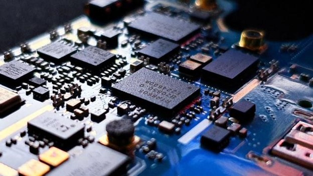
Selecting the right components is crucial in PCB design. The components should be chosen based on the required functionality, size, and cost. It’s also important to ensure that your selected components are available in the required quantities at the right time. The component placement should be such that the traces connecting them are as short as possible. The shorter the traces, the lower the chances of signal interference.
Follow Good PCB Design Rules
Design rules are guidelines that ensure the PCB design meets your specifications. The rules dictate the minimum trace widths, clearances between traces and pad sizes. Following these rules ensures that the design is manufacturable and reduces the chances of errors. Some of the design rules we pay close attention to are trace width, spacing between traces, and clearance from the edge of the board.
Use Copper Pours
Copper pours are areas of copper that are connected to a ground or power plane. These areas help to reduce electromagnetic interference (EMI) and improve the overall signal integrity. Copper pours are also useful in dissipating heat from components. Our team places the copper pours in the right locations to not interfere with other signals on the board.
Minimize Vias
Vias connect traces from one layer to another. However, too many vias can increase the chances of signal interference and reduce the manufacturability of the board. Minimizing the number of vias and keeping them as small as possible helps to ensure that the design meets the required specifications.
Check the PCB Design for Errors
It’s important to check the PCB design for errors before sending it for manufacturing. Errors such as short circuits, incorrect component placement, and incorrect trace routing can cause significant problems in the final product. There are many testing procedures and software tools we use to check for design errors.
Optimize for Manufacturability
Optimizing the PCB design for manufacturability helps to reduce the chances of errors and ensures that the board can be manufactured at a lower cost. Some of the factors to consider when optimizing for manufacturability include the board size, the number of layers and the type of components used.
PCB design is a crucial aspect of electronics design, and an efficient PCB design layout can help to minimize errors and reduce costs. The above tips and tricks are just some of the ways that Sonic Manufacturing Technologies will ensure an efficient PCB design layout. Our goal is to design high quality PCBs that meet your required specifications and are manufacturable at a lower cost. Contact us today for a free quote.